 133-9291-8466


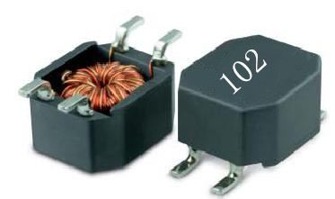
Let's talk about the design factors of the mold inductance.
 31/01/2019
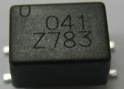
On some motherboards, we can see the common mode inductor, but on most motherboards, we will find that the component is omitted, and even some locations are not reserved. Is such a motherboard qualified?
It is undeniable that the common mode inductor has a good suppression effect on the common mode interference of the high-speed interface of the motherboard, which can effectively prevent the EMI from forming electromagnetic radiation through the cable and affect the normal operation of the remaining peripherals and our physical health. But it is also worth noting that the EMI design of the board is a fairly large and systematic project, and the design of the common mode inductor is only a small part of it. The high-speed interface has a common-mode inductor design board, and it is not good to have an overall anti-EMI design. Therefore, from the common mode filter circuit we can only see one aspect of the board design, which is easily overlooked by everyone, and it is a mistake to see the wood.
Only by understanding the overall anti-EMI design of the board can we evaluate the advantages and disadvantages of the board. So, what do the excellent board design generally do in terms of EMI prevention?

1. Motherboard Layout design
For good motherboard layout design, most of the clock traces will be shielded or close to the ground to reduce EMI. For multi-layer PCB design, the open-loop principle is adopted in the adjacent PCB trace layer, and the wires are layered to one layer, which avoids the formation of loops in the design. If the trace forms a closed loop, it acts as an antenna and enhances the EMI radiation intensity.
The unequal length of the signal line will also cause the impedance of the two lines to be unbalanced to form common mode interference. Therefore, in the design of the board, the signal lines will be treated in a serpentine manner to make the impedance as uniform as possible, and the common mode interference is weakened. . At the same time, the serpentine line also minimizes the curved swing during routing to reduce the area of the annular region, thereby reducing the radiation intensity.
In high-speed PCB design, the length of the trace is generally not an integer multiple of 1/4 of the wavelength of the clock signal, otherwise resonance will occur, resulting in severe EMI radiation. At the same time, the routing should ensure that the return path is minimal and smooth. For the design of the decoupling capacitor, it should be set close to the power pin, and the area surrounded by the power supply trace and ground of the capacitor should be as small as possible to reduce the ripple and noise of the power supply and reduce the EMI radiation. .
Of course, the above is only a small part of the principle of PCB anti-EMI design. The layout design of the motherboard is a very complicated and profound knowledge. Even many DIYers have the consensus that the layout design is excellent or not, which has a very significant impact on the overall performance of the motherboard.
2. Cutting off the motherboard wiring
If you want to completely isolate the electromagnetic interference between the motherboard circuits, this is absolutely impossible, because we have no way to "package" the electromagnetic interference one by one, so we must use other methods to reduce the degree of interference. The metal wires in the motherboard PCB are the culprit in the transmission of interference currents. They transmit and emit electromagnetic interference signals like antennas, so "cutting off" these "antennas" in appropriate places is a useful way to prevent EMI. The "antenna" is broken, and it is surrounded by a ring of insulators, and its interference to the outside world is naturally greatly reduced. If the filter capacitor is used at the disconnection, the electromagnetic radiation leakage can be further reduced. This design significantly increases the stability of high frequency operation and prevents the generation of EMI radiation, which is used by many large motherboard manufacturers.
3. The design of the motherboard interface
I don't know if you noticed that the motherboard will be accompanied by an open thin iron strip. In fact, this is also used to prevent EMI. Although the EMI shielding performance of the chassis is good, the electromagnetic wave will leak from the opening of the chassis surface, such as the PS/2 interface, USB interface, and the opening of the serial port. The size of the hole determines the degree of leakage of electromagnetic interference. The smaller the aperture of the opening, the greater the degree of attenuation of the electromagnetic interference radiation. For a square hole, L is the diagonal length.
After the blank is used, the metal contacts on the blank and the input and output parts of the motherboard are well grounded through the chassis, which not only attenuates EMI, but also reduces the size of the square hole and further reduces the L value. More effectively shield electromagnetic interference radiation.
The above three points are just a few of the main anti-EMI designs in the motherboard design except for the circuit design. It can be seen that the anti-EMI design of the motherboard is a whole concept. If the overall design is unqualified, it will bring a large electromagnetic Radiation, and these are not compensated by a small common mode inductor.
 133-9291-8466
 semcms
 13392918466